Abstract Electrically conductive polymers: structure, properties, application. Organic bioelectronics: how electrically conductive polymers help combine electronics and living tissue Conducting polymers are the basis of 21st century electronics
Article for the “bio/mol/text” competition: Scientists have long dreamed of turning animals and plants into cyborgs controlled by electrical signals, and are trying to do this in a variety of ways. So, about 10 years ago, a new scientific field appeared - organic bioelectronics - in which electrically conductive polymers act as intermediaries between living beings and computers. Remote control of the color of rose leaves, an artificial neuron and targeted pain treatment - the first results of this triple alliance are already impressive.
Sponsor of the nomination - .
The general sponsor of the competition, according to our crowdfunding, was an entrepreneur Konstantin Sinyushin, for which he has great human respect!
The sponsor of the audience award was the Atlas company.
The sponsor of the publication of this article is Andrey Aleksandrovich Kiselev.
All living organisms are little bit robots or computers. Only instead of the usual electricity - electrons running through wires to the outlet and back - we are controlled by nerve impulses, streams of charged molecules called ions. And the “buttons” in living electrical circuits are pressed not by fingers, but by special substances - neurotransmitters. When their concentration exceeds a certain limit, a chain of biochemical reactions begins in the cell membranes of neurons, which ends with the excitation of a nerve impulse.
Now scientists are trying to “marry” the computers inside us with the usual silicon chips: brain-computer interfaces are already able to recognize the activity of nerve cells and convert them into meaningful commands for electronics. So, using the power of thought, you can play simple games, move a robotic prosthetic arm, or even control a quadcopter. However, all these devices still suffer from errors and inaccuracies - it is not easy to combine electronic and ionic currents in one device.
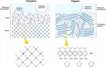
Electrically conductive polymers, which simultaneously conduct both types of current (Fig. 1), can become “translators” from the living language to the language of microcircuits. Discovered in the 70s of the last century, these materials were actively studied by many scientists: they were used to make transistors, solar cells, organic light-emitting diodes (OLED) and other organic electronics devices.

Figure 1. Schematic representation of organic ( right) and inorganic ( left) semiconductors in contact with an electrolyte. The sizes of charged ions are much larger than the distances between atoms in inorganic semiconductors and therefore ionic conductivity is impossible in these materials. At the same time, the characteristic sizes of voids between the chains of macromolecules of conjugated polymers are comparable to the sizes of hydrated ions and therefore ionic conductivity is possible in this class of compounds.
Now the advantages of electrically conductive polymers - flexibility, simplicity and variability of synthesis, as well as biocompatibility and ionic conductivity - are being used by organic bioelectronics - a very young field of materials science, which already has something to boast about.
Diagnostics from the inside
The operation of many brain-computer interfaces is based on taking an EEG: a cap with electrodes is attached to a person’s head, in which, under the influence of ionic currents flowing in the brain, their own electronic currents arise. In a 2013 paper, scientists from France proposed using organic electrochemical transistors for the same purposes.
Conventional semiconductor transistors are the main components of all electrical logic circuits, a kind of electronic buttons with three contacts. The relatively large current flowing through them from one contact to the other can be controlled by a small signal (much less current or voltage in the case of a field-effect transistor) applied to the third contact. By collecting many transistors in one circuit, you can amplify, attenuate and convert any electrical signals or, in other words, process information.
Organic transistors, with which researchers recorded epileptic activity in living laboratory mice, work in a similar way. The third control contact in this transistor was made of a conducting polymer and inserted directly into the brains of rodents. The polymer changed its structure (and, as a result, conductivity) along with fluctuations in the electrical activity of nerve cells, and as a result, even small characteristic changes in ionic currents in the “cyborg” brain led to noticeable differences in the current flowing from the input contact of the transistor to the output (Fig. 2 ).

Figure 2. In vivo recording electrical activity of the brain using organic transistors. Pink The color shows the dependence taken using an organic electrochemical transistor, blue- plastic electrode, black- metal electrode. Please note that the last two electrodes register the electrical signal by potential jumps, and the transistor - by current jumps in the electrically conducting channel.
In their experiment, the French showed that organic transistors make it possible to record the electrical activity of the brain much more accurately than their modern inorganic counterparts. In experiments by other scientific groups, organic transistors are successfully used to take ECGs or, for example, determine the concentration of lactic acid, glucose and other biomolecules.
Plastic neurons
Today, neurological and psychiatric diseases are treated mainly with the help of medications, but it can be very difficult to select their dosage, target delivery of the drug to certain cells, and at the same time take into account its side effects on a variety of processes in the body. A large team of Swedish scientists from several institutes proposed solving these problems using the same electrically conductive polymers, or rather, using another organic bioelectronics device - an organic electron ion pump capable of pumping ions from one medium to another.
In their work, the researchers studied laboratory rats in which they first induced neuropathic pain (its cause was not an external irritant, but the disrupted functioning of the neurons themselves), and then treated it with a targeted injection of a neurotransmitter GABA (gamma-aminobutyric acid), which reduces irritation of the central nervous system. A miniature organic pump (about 12 cm in length and 6 mm in diameter) was inserted into the spinal cord of rats, and its reservoir was filled with GABA (Fig. 3). With the application of an external electrical voltage, GABA molecules began to exit through four ion-conducting polymer channels into the intercellular space (video 1).

Figure 3. Implantable organic electrochemical pump. A - photograph of the device, B - schematic representation of the device, on the left - electrical contact, in the center - a reservoir with GABA, on the right - excretory channels. The total length of the device is 120 mm, the diameter of the tank is 6 mm. C - four organic electrochemical outputs are located at the points where the branches of the sciatic nerve enter the spinal cord.
Video 1. Organoelectronic ion pump
As a result, the rats lost pain (this was checked using a tactile test: elastic threads of varying stiffness were applied to the paws of the rats and the pressure at which the animal would withdraw its paw was monitored), and no side effects were observed. With all other methods of treating neuropathic pain using GABA, the drug is injected into the spinal cord in a large dose, which is distributed throughout the nervous system and, in addition to suppressing pain, leads to walking disorders, lethargy and other side effects.
In parallel with this work, the same group of researchers made the first polymer-based artificial neuron. It combined an ion pump with biosensors sensitive to glutamic acid(the most common excitatory neurotransmitter) and acetylcholine(a neurotransmitter that transmits a signal from neurons to muscle tissue). For example, in one of the experiments, a “plastic” neuron monitored the level of glutamate in a Petri dish, and when a certain threshold was exceeded, a current was excited in it, which opened the reservoir of the ion pump, releasing acetylcholine into the environment.
The operation of an artificial neuron is very similar to how real ones function: a nerve impulse is excited in one of them and runs through the entire cell to the point of contact with another neuron, where glutamic acid is released, which, as it were, presses a button and excites the next neuron (Fig. 4) . So, along a chain of neurons, the impulse reaches the muscle cell, which is no longer excited by glutamic acid, but by acetylcholine. The plastic neuron created by the Swedes may well repeat these actions and transmit signals to other cells. In the experiment, these were SH-SY5Y neuroblastoma cells, the activation of which was monitored by characteristic increases in ion concentration upon binding of acetylcholine receptors.

Figure 4. The scheme for converting a chemical signal into an electrical signal and back in an artificial polymer neuron is identical to the scheme for the operation of a living neuron. Biosensor ( represented in green) responds to an increase in the concentration of one neurotransmitter ( orange dots), which generates a flow of electrons that excites the organic electrochemical pump ( represented in blue), releasing another neurotransmitter ( blue dots).
From electronic roses to the greenest energy
Research on mice, rats and other laboratory animals must be approved by ethics commissions, and therefore the most daring experiments in organic bioelectronics are easier to carry out on plants. So, at the end of 2015, the same Swedish group made the first cyborg rose. True, it can’t do anything spectacular yet - neither open up at the press of a button on the control panel, nor change its color depending on the humidity of the environment, nor take over the world, but the researchers did manage to do something interesting.
In the first experiment, a cut rose was placed in water with a dissolved electrically conductive polymer, which rose up the cutting and formed a conductive channel in the rose. Next, the scientists connected electrical contacts to the ends of the channel and inserted a control electrode - a gold wire coated with a conductive polymer - into the handle. This is how a kind of organic transistor was assembled inside the rose. In this case, it was possible to connect several control electrodes to one channel at once and make a simple logic circuit through which current flows only when certain control voltages are applied to both gold wires.
In the second experiment, an aqueous solution of another electrically conductive polymer, which can change color when an external voltage is applied, was pumped into rose leaves using a syringe. Electrodes were applied to the leaf, the current was turned on, and voila: the veins of the leaf acquired a bluish-green tint. It was the polymer pumped into them that turned from colorless to blue (video 2). At the same time, when the tension was removed, the leaf again became a healthy green color.
Thus, scientists have shown that with the help of simple technology it is possible to create simple electronic circuits inside plants. In the future, this will make it possible to control their physiology and, for example, achieve increased productivity without genetic modifications or even make tiny power plants using the energy of photosynthesis. Of course, for now this sounds too expensive, but someday organic bioelectronics technologies will allow targeted control of each plant, and not the entire population at once.
Bioelectronic future
The first experiments showed that organic bioelectronics devices are quite capable of receiving, transmitting and processing bioelectric signals. What's next? Now they have learned how to make polymer materials biocompatible and biodegradable, and therefore any living organism can literally be stuffed with chips based on them. All that remains is to teach them wireless information transfer, and inside the human body it will be possible to create a local network of sensors that constantly monitor various medical indicators such as glucose levels, heart rate and electrical activity of selected neurons, and then transmit their signals to implanted medical robots based on the same ionic pumps so that they begin to deal with the problem.
If the idea of becoming such a cyborg is not at all to your liking, you can simply swallow a tablet with a built-in flexible microcircuit - based on the acidity, temperature and concentration of various substances, it will accurately calculate where to release the medicine, and, having done a good deed, will simply be digested inside us as some piece of sugar.
HISTORICAL EXCURSION
Polymers with high electrical conductivity, pseudometallic and semiconducting properties were obtained back in the 60s. A classic example of a polymer of this class is polyacetylene. Thanks to polyconjugated chemical bonds, its electrical conductivity can be changed over a wide range both during the synthesis process (by controlling the length of the polymer chains) and under field influences (thermal, electromagnetic, ionizing radiation), leading to a corresponding change in either the primary structure of the polymer (structural rearrangement) , or to a change in the degree of its polymerization. Conducting polymers are widely used for the manufacture of electrodes for chemical current sources (polyanilines), automatic thermostats and voltage stabilizers (polyacrylonitriles), as electrolytes for capacitors (polypyrolle salts), etc. The discovery and study of the effect of photoconductivity in polynitriles, polyphthalocyanines, polyphenyls and polyphenylenevinylenes led to the formation of photodetectors based on them, and the high “sensitivity” of the spectral characteristics of polymers to the original structure and polymer component made it possible to create devices with a wide spectral range. True, in fairness, it should be admitted that their luminescence quantum yield did not exceed several percent. In the 1980s, as a result of studies of conducting polymers with a high degree of orientation of polymer chains in a bulk sample (which makes it possible to use the characteristics of the quasi-one-dimensional structure of macromolecules), quasicrystalline polymer materials with high anisotropy of electrical characteristics were obtained. The mobility of charge carriers in them reached 5000–6000 cm2/V.s.
The variety of structures of polymer systems and the possibilities of their modification have provided researchers with a wide range of material characteristics. This, naturally, prompted them to try to implement active electronic devices based on polymer materials. The work was carried out on the basis of the theory of semiconductor devices, physical and technological principles of their formation, which had been fairly well developed by that time. At the same time, in polymer (molecular) systems, the analogue of the Fermi level was the energy states of carriers at the highest and lowest unoccupied levels of molecular orbitals, and the analogue of the doping process, leading to a change in the position of the Fermi level, was the chemical substitution operation, causing a change in the ionization potential and electron affinity . By changing the primary structure of a polymer, it is possible to set the levels of molecular orbitals and, consequently, the width of its band gap. Continuing the consideration of analogies, we point out that systems of linear polymers with conjugated bonds can be used as interconnects.
After a brief historical excursion, we will consider the “advancement” of polymers into the world of modern electronic devices.
ORGANIC LEDS WITH HIGH BRIGHTNESS
The first polymer-based electronic devices were light-emitting diodes (LEDs). Now we can assume that developments have almost reached a level that allows us to move on to the industrial production of organic LEDs, and the task of today comes down to creating devices with high brightness. Numerous studies in this area in various ways have led to the optimal design and technological option, which is called the “transparent organic light emitting diode” (TOLED, Fig. 1). Its operating principle is extremely simple and consists in the generation of radiation by polymer molecules under the influence of an electric field as a result of the recombination of carriers in the electroluminescent layer. Structurally, the LED must be designed so that the transparent electrode, hole transfer layer, electroluminescent layer and waveguide are as transparent as possible, and the electron transfer layer and negative electrode provide maximum interference and specular reflection of the radiation. To enhance the contribution of reflected radiation in some LED designs, the negative electrode is given an appropriate shape (for example, a concave parabolic mirror) and optical elements based on Fresnel lenses are introduced into the plastic layer.
New organic materials for LEDs are currently being actively studied. Thus, at Fujitsu, based on a copolymer of para- and metabutadiene, a conductive polymer with maximum radiation intensity was obtained with a ratio of para- and meta-modifications of 2:1. A conductive polymer based on thiophene is used as a hole-injecting layer, which makes it possible to reduce the operating voltage of LEDs at high current values. The positive electrode, made of Mg–In alloy, is highly stable and provides a high level of electron injection. A negative indium tin oxide electrode is applied to a glass substrate.
In the future, the company plans to use this organic LED with polysilicon field-effect thin-film transistors to create displays capable of reproducing “live” images. These displays will have high brightness and a wide viewing angle, and their cost will be significantly lower than that of currently produced AM LCD displays.
DISPLAY SYSTEMS
Until recently, LEDs based on organic compounds were used only in cell phones and watches, since there were significant technological problems in maintaining the properties of LEDs when forming matrices. The development of “low temperature” technologies has removed this obstacle. The intensity of work and the range of tasks being solved to create flat indicators and displays based on organic materials are evidenced by research in the field of obtaining tunable color LEDs with a vertical structure (Princeton University) and a color organic EL display for wall-mounted TVs and mobile multimedia systems (Idemitsu Kosan company) , as well as the development of pilot production of polymer LEDs based on the technology of Cambridge Display Technology (Uniax) and the production of LCDs on plastic substrates (Ricon). The luminous efficiency of modern organic LEDs and information display devices based on them is 10–60 lm/W, the brightness of light radiation reaches 50,000 cd/m2, and the resource is 10 thousand hours (at a brightness of 150 cd/m2).
The main achievement of the 90s was the development of organic blue LEDs, which made it possible to move on to the creation of full-color screens based on RGB triads. One of the main technological problems in this case is the damaging effect of technological processing processes during the formation of a set of LEDs (the first elements of the set are chemically affected during the formation of the second, and the first two are affected by the manufacturing process of the third element of the set). The presence of even minor chemical contaminants (especially alkali metals) can lead to significant degradation of the properties of the electroluminescent material and cause significant changes in the glow intensity and spectral characteristics, reducing the service life of the device. Masking technology for protecting layers during the sequential production of triad elements inevitably leads to a limitation in the resolution of the display.
This problem has been successfully solved by moving to maskless technology for manufacturing a three-dimensional rather than planar structure. Using this technology, triad elements are made in the form of three- or tetrahedral pyramids, formed by pressing on a plastic substrate. An organic material is applied to a certain face of all pyramids of the matrix using directed vapor deposition, providing radiation of the same color. Then the substrate is rotated at the appropriate angle (120° or 90°), and the material of the next luminescent color is deposited. On the fourth side, a layer of one of the colors of reduced brightness is formed, which allows you to expand the color gamut reproduced by the display, as well as stabilize the white balance during operation. This design provides an almost threefold increase in resolution. A polymer layer with pyramids and contact holes is applied on top of an active matrix addressing circuit on thin-film field-effect transistors (TFTs), manufactured together with pillar leads on a glass substrate. All components of the technological route have already been worked out, and the developers hope to produce fairly cheap displays with high performance.
The development of ultra-thin organic displays is of undoubted interest. The Massachusetts Institute of Technology has developed a technology for producing displays on a layer of plastic only 100 microns thick, which can be rolled into a roll with a radius of 5 mm without changing its properties. The image is formed in a layer of electrophoretic paste applied to a grid of electrodes on a flexible polymer substrate. The paste consists of microcapsules containing white (titanium dioxide - a standard component of ordinary white) and black (a mixture of organic dyes) microparticles suspended in molten polyethylene. The capsule shell undergoes special treatment to ensure its transparency. The average capsule size is about 50 microns. A grid of transparent electrodes is applied on top of the paste layer. When a voltage of one polarity is applied, negatively charged white particles move to the top of the capsules and block the black particles. As a result, the capsule becomes white. When the polarity changes, the white particles move to the bottom of the capsule and its color becomes black. The resolution of such a display determines the pitch of the electrode grid, and already for the first samples it was comparable to standard values for laser printers. The power consumption of a display with a screen diagonal of 30 cm is 12 mW, the duration of information reproduction when the voltage is removed is not limited (until new addressing). The image can be changed more than 107 times without performance degradation. Based on this design, it is possible to create “electronic paper”.
Xerox announced the preparation of copiers based on “electronic paper” - ultra-thin displays made using Gyricon technology, which involves the use of oil cavities with plastic spheres. When voltage is applied, the spheres are oriented relative to the surface with either the black or white side. To reproduce the image, two AA batteries are enough. Correction and updating of information is allowed. The only drawback of displays is the need for protection from electrical interference, in particular from static electricity. “Electronic paper,” just like regular paper, is light, flexible, and easy to read from any angle. In addition, it has such new properties as the ability to update information several thousand times and use an electronic pointer. According to Xerox specialists, the price of such paper will not exceed 25 cents per A4 sheet.
ORGANIC THIN FILM TRANSISTORS
When manufacturing displays, the joint formation of TFTs using traditional technology and organic LEDs is difficult due to high-temperature processes that cause degradation of the properties of organic materials. TFTs based on organic materials can be manufactured at lower temperatures and at the same time use cheap plastic substrates instead of expensive glass, which will significantly reduce the cost of the entire product. The development of organic TFT technology opens up great opportunities for creating ultra-light and ultra-flat displays with high flexibility and strength. Solving the technological issues of producing TFTs based on organic materials will make it possible to produce all display elements using similar technological processes, which will reduce production costs and reduce the heterogeneity of the equipment used. In terms of their characteristics, modern organic TFTs are not inferior to standard ones based on amorphous silicon films. The typical structure of organic TPT is shown in Fig. 2.
A prototype TFT based on pentacene with a gate length and width of 5 and 500 μm, respectively, and a gate dielectric thickness of 140 nm had a threshold voltage of 10 V and a saturation drift mobility of 1.7 cm2/V.s (a record result for organic transistors). To reduce the leakage current between individual TFTs, a specific Corbino topology is used, in which the source electrode forms a closed ring around the active region of the TFT, in the center of which the drain electrode is located. With this design, the gate controls all current flowing from drain to source, resulting in an on-to-off current ratio of ~108, as well as low leakage currents (the off-state current is close to the noise level).
Thus, it can be stated that today the technological problem of forming information display devices entirely from organic materials has been solved.
OPTOELECTRONICS AND LASER ENGINEERING
Advances in the creation of organic LEDs and information display systems also stimulate the development of devices with electrical excitation based on organic polymers, one of the most promising materials for the manufacture of new types of optoelectronic ICs. The main advantages of such ICs are low cost and fairly simple technology suitable for mastering mass production. Research in this area is carried out by many companies in the USA, Germany, Austria and Italy. And today, industrial polymer light guides are already used in standard hybrid optoelectronic circuits.
More than a dozen polymers with semiconductor properties suitable for laser generation in the entire visible range have been studied. Of particular interest to developers are conjugated polymers with side chains, since it is the side chains that determine the width of the energy band, i.e. radiation wavelength. Due to the high extinction of the generated radiation (films only 0.1 μm thick absorb 90% of the radiation), the weak dependence of the quantum efficiency of photoluminescence on the amount of active polymer in the resonator and the large energy shift between the absorption and emission spectra (which makes it easy to achieve population inversion), conjugated polymers Even at small thicknesses they are suitable for forming the active medium of a laser. The high solubility of conjugated polymers with side chains in conventional organic solvents greatly simplifies the technology of deposition and formation of the necessary layered film topological structures, including traditional photolithography methods, well established in microelectronics.
One of the most serious problems in manufacturing devices with electrical excitation on polymer films is the high density of the threshold generation current (~1 kAh cm2). It is solved by introducing distributed feedback and a distributed Bragg reflector (DRB) in order to increase the quality factor of the resonator. The ROB performs the function of a resonator mirror. It is formed by alternating polymer layers of varying thicknesses with low and high refractive index values. Since the cavity length varies depending on the radiation wavelength, a ROB with a similar structure can support multimode lasing.
An example of the successful use of polymers in laser technology is the first electrically excited organic laser from Lucent Technologies, suitable for industrial production. It is made on tetracene crystals, the molecules of which contain four benzene rings. The field structure (a channel 25 μm wide and 200–400 μm long) was created on tetracene layers 1–10 μm thick, obtained by deposition onto a dielectric substrate from the vapor phase in an inert gas flow. A layer of aluminum oxide 0.15 μm thick was used as a dielectric, and the control electrodes were made of zinc oxide doped with aluminum. The structure is a planar multimode waveguide with total internal losses of ~100 cm-2. The laser cavity was formed by cleaving a tetracene crystal to form faces with a reflectance of ~8%. At a high density of injection current in the resonator, channeling of radiation at a wavelength of 575.7 nm was observed with amplification when operating in a multimode mode. At room temperature, the laser operated in pulsed mode, and at 200K - in continuous radiation mode. By reducing reflection losses due to the introduction of distributed feedback and ROB, operation in continuous mode and at room temperature is possible. The advantage of the laser is the possibility of frequency tuning, since the emission spectrum of tetracene is quite wide.
Lasers based on organic materials are much cheaper than semiconductor lasers, and a wide selection of materials allows them to cover a significant spectral range. We can confidently predict that such lasers will find wide application in optical memories and laser printers in the near future.
INDUSTRIAL DEVELOPMENT OF POLYMER TECHNOLOGY
Despite the heterogeneity of the polymer materials used, most operations for creating devices and structural elements are similar in structure and can be largely unified. Such operations, first of all, include the processes of deposition (application) of polymer layers and shaping processes. It was already indicated above that for most thin- and thick-film materials, the well-established processes of vapor deposition, screen printing and lithography (for soluble compositions) can be used.
A revolutionary approach to the development of technology for mass production of electronic devices based on organic films was demonstrated by the Californian company Rolltronics. According to its technology, called roll-to-roll (from reel to reel), the production conveyor cycle uses a large reel with flexible plastic, which plays the role of a substrate for the future device (Fig. 3). The length of the plastic tape is more than 300 m, and the width can exceed 1 m. Consecutive application and formation of layers is carried out in specialized processing chambers that ensure the entire technological cycle. The developers believe that they will be able to form structures at temperatures no higher than 100–125°C, which will allow the use of most modern polymer materials.
Together with Iowa Thin Film Technologies, Rolltronics planned to launch a roll-to-roll production line by the end of 2001. The main element of future designs – a thin-film transistor – was chosen as a “test of the pen”. In addition to TFTs, the company intends to produce memory circuits, power devices and display elements, as well as all components of electronic books and electronic paper. Roll-to-roll technology is suitable for the formation of flat screens, lighting and information LED panels, solar cells, optoelectronic devices and semiconductor lasers. Representatives of the company call this technology a breakthrough into the future, emphasizing its extremely high efficiency and productivity, which will allow us to move to mass production of new types of electronic devices and sharply reduce their cost.
DEVELOPMENT PROSPECTS
The physical principles and technology used are "polymer electronics" - the first natural step towards molecular electronics. This is explained by the fact that, unlike classical solid-state electronics, where the properties of a crystalline body are considered and active structures are formed in its volume, in the case of using polymers it is necessary to take into account the properties of molecules. In the transition to true molecular electronics, when the active elements are already single molecules, the main task is the choice of a technological method of point (local) influence on the molecule and changing its primary chemical structure. Naturally, if a technological tool is not capable of locally modifying the original molecular system at the atomic level, methods of its self-construction and self-regulation should be developed, as happens in nature in the life cycle of viruses and bacteriophages. To a first approximation, these include the Langmuir-Blodgett method for producing monolayer films or the method of self-assembled monolayers of oligomers on a metal substrate (Self-assembled monolayers - SAM). These methods can be conditionally, by analogy with the technology of solid-state devices, classified as “single-layer” epitaxy.
One of the options for the transition to molecular electronics is “hybrid” technology, when “molecular elements” are used using classical electronics methods. An example of such a combined technology is IBM's proposed design use of carbon nanotubes to create transistors that are 500 times smaller in size than modern silicon devices. In addition, in the absence of oxygen, they are able to withstand heating up to 1000°C.
Modern tools for modifying and monitoring atomic structures - atomic force microscopy (AFM) and scanning tunneling microscopy (STM) - can provide technological requirements at the atomic level. But unfortunately, both AFM and STM are sequential methods with not very high throughput, and in the near future they will only be used as a laboratory tool. However, it was with the help of AFM and STM that molecular electronics devices were first successfully created. These methods make it possible to solve the most difficult task of assembling molecular electronic devices – the formation of contacts. Theoretical models of AFM and STM methods for forming structures and measurements are still developing, and many more discoveries can be expected here. However, the implementation of molecular electronics methods suitable for industrial development is a matter of the future.
CONCLUSION
All of the above shows that electronics is on the threshold of a “polymer” revolution. In the next three to five years, it will be possible to “print” electronics products as wallpaper. Such plastic “wallpapers” will be used to create full-color screens and displays, solar panels and white LED lighting panels, electronic paper and much more. New electronics products based on polymer materials, which will appear in the next decade, will revolutionize the operating conditions of electronic equipment, expand the capabilities of information technology, and create the preconditions for the transition to new principles of organization, learning, life and entertainment. The task of Russian electronics is not to miss this breakthrough and to join in the development of polymer electronics in a worthy manner.
Literature
Laser Focus World, 2001, v.37, no. 3, p. 41–44.
Semiconductor International, 2000, v.23, no. 8, p.46.
Semiconductor International, 2001, v.24, no. 6, p.50.
Semiconductor International, 2001, v.24, no. 8, p.40.
Solid State Technology, 2000, v.43, No. 3, p. 63–77.
Photonics Spectra 2000, v.34, no.5, p.44.
Journal of American Chemical Society, 2000, v.122, No. 2, p. 339–347.
Foreign electronic technology, 2000, issue 1, p. 66–72.
This article is devoted not to composite conductive polymers, in which high electrical conductivity is achieved due to the properties of the filler, but to conductive polymers with their own electrical conductivity.
Report on achieving a metallic level of conductivity when doping polyacetylene (PAc) films, published Shirakawa et al . (1977) generated enormous interest in the study of conductive polymers, which continues to this day. Although this was not the first example of a conducting polymer, the increase in electrical conductivity by more than 10 7 times when trans-PAC was doped with arsenic or iodine pentafluoride was dramatic and significant (Fig. 1). This discovery sparked a surge of interest in conducting conjugated polymers due to the prospect of increasing their electrical conductivity.
Rice. 1. Increase in the electrical conductivity of trans-PAC upon doping with arsenic pentafluoride.
In the 1960s, other members of the class of conducting polymers polyaniline and polypyrrole were studied and their electrical conductivity was found to be 330 Ohm -1× m -1 and 754 Ohm -1 × m -1, respectively.
Theory of electrical conductivity of conducting polymers.
After the discovery of the metallic properties of PAC, most theoretical work was carried out using this conducting polymer as an example. In the first works Longuet - Higgins and Salem (1959) and a number of others used the Hückel model, and it was shown that the PAC chain in the ground state has a structure with alternating bonds (Fig. 1, b), and not a structure with equal lengths of C-C bonds (Fig. 1, a ).

Rice. 2. Chemical structure of trans-polyacetylene with equal bond lengths (a) and alternating bonds (b).
In 1979, the Hückel model of strong binding was proposed, which served as the basis for the analysis of the molecular and electronic structure of PAC and is now usually called the model SSH.
There are two possible phases of alternating bonds, which means the existence of two alternative structures for the ground state of the polymer, I and II in Fig. 3, whose energies are degenerate. These structures are characterized by a bond alternation parameter that takes values of ±1. Note that the value of the bond alternation parameter equal to zero corresponds to a structure with equal bond lengths. If two sections of the target have opposite values of the connection alternation parameter, a defect appears in the place where this parameter changes sign, as shown in Fig. 3, and the unpaired one turns out thereπ -an electron that is not included in a double bond in any part of the chain.

Rice. 3. Two possible types of alternation of bonds in PAC and the formation of a soliton.
The polymer chain as a whole is electrically neutral, but the electron at the junction (kink) has an unpaired spin.π -The electrons of double bonds have paired spins, so an ideal polymer chain is diamagnetic, while a chain with a kink is weakly paramagnetic. Since the energy of the chain on both sides of the kink is the same, it can move along the chain, and the total energy does not change, i.e. An unpaired electron is a mobile object that can move freely along the chain. By analogy with single ( solitary ) waves in water, such a formation is called a soliton.
With an odd number of carbon bonds in the ring, a soliton should appear, since the first and last bonds should both be single or double. If the number of bonds in the ring is even, the boundary conditions are satisfied and the soliton does not arise. However, in a ring with an even number of bonds, two solitons of opposite signs can arise, a soliton and an antisoliton, when the violation of the alternation of bonds that formed the antisoliton compensates for the violation of the alternation of bonds that led to the formation of the soliton. These considerations are also applicable to a chain of finite length, in which the end groups fix the phase of alternation of bonds. Thus, the ground state of a chain of finite length, at the ends of which the phases of alternating bonds are opposite, must contain a soliton, otherwise a soliton will not form.
When polyacetylene is doped with strong electron acceptors or donors, the formation of charged soliton states requires less energy, which leads to an increase in the electrical conductivity of the polymer.
Electrical properties of conductive polymers.
Synthesis methods by polyaddition and polycondensation can be used to obtain conducting polymers.
The above experimental data indicate that the band gap between the valence band and the conduction band in conducting polymers is several electron volts, which is comparable to the band gap in silicon and germanium. In this case, the band gap is much larger than the energy of thermal motion at room temperature (~ 0.025 eV), so the number of thermally excited charge carriers under these conditions is very small. Correspondingly, the intrinsic conductivity of pure conducting conjugated polymers is also small. The same picture occurs for silicon and germanium, for which it is necessary to introduce small amounts of acceptors or donors (dopants or dopants) in order for the impurity conductivity to reach the level required for practical use. However, the electrical conductivity of freshly prepared conducting polymers often turns out to be higher than the level of their own conductivity, which is the result of accidental doping of the polymer with catalyst residues, oxidative or reducing impurities that entered it during synthesis or during subsequent manipulations. The most common impurity is oxygen. The effect of random doping can be neutralized by chemical treatment, since most random doping is caused by oxidative impurities, resulting in a p-type semiconductor; treatment with reducing agents leads to a decrease in electrical conductivity.
Maximum electrical conductivity is observed in pure oriented polymers with high molecular weight. The largest values obtained are ~10 7 Ohm -1 m -1 for PAC ( Tsukamoto, 1992) and 2 × 10 5 Ohm -1 m -1 for polyaniline ( Pomfret et al ., 1998). Electrical conductivity per unit mass is close to or higher than the values characteristic of normal metals, since the lower density of polymers compensates for the lower electrical conductivity. The work function of metallic polymers is close to the values for normal metals, for example, for polyaniline it is 4.8 eV, and for PEDOT - ~5 eV, which is an intermediate value between the values for gold and aluminum.
Literature:
Blythe E.R., Bloor D. Electrical properties of polymers. Per. from English - M: FIZMATLIT, 2008. - 376 p.
If it is an exaggeration to say that organic and printed circuits are revolutionizing microelectronics, it is a very small one. Never before has the time gap between fundamental research and its practical application been reduced at such a rapid pace. Therefore, this topic was one of the main ones at the international specialized exhibition of plastics and rubber “K-2013” (October 16–23, 2013, Dusseldorf), at which a special innovative section of the exhibition - Printed Electronics - provided visitors with ample opportunities to get acquainted with printing technologies , functional surfaces, RFID solutions, flexible displays, as well as OLED developments.
Over the past ten years, the world has been experiencing a boom in the development of organic and printed electronics; Hundreds of companies and research institutes are racing to capture the new market, which is growing exponentially (see figure) and is predicted to increase by an order of magnitude within ten years.
It is believed that the history of this scientific direction began in 1977, when chemists Alan Heeger, Alan McDiarmid and Hideki Shirakawa published the results of their research, which showed that halogen-modified polyacetylene can conduct electric current almost like a metal. This discovery and other fundamental research in the field of organic polymers contributed to the development of organic electronics, which combines developments in solid state and molecular physics, organic and inorganic chemistry, polymer materials science, electronics and printing. In 2000, the founders of this breakthrough direction received the Nobel Prize in Chemistry “for the discovery of conductivity in polymers.”
New features
In the name of the new generation of microelectronics - the so-called organic and printed electronics - the term "organic" is used for the simple reason that tiny circuit boards with myriads of transistors, sensors, LEDs and connecting circuits are no longer built on the basis of silicon and gallium arsenide, but on the basis carbon derivatives. The term "printed" means that they can be applied to lightweight, flexible and even transparent substrates that are wound directly from rolls using widely used printing methods (screen, inkjet or flexo printing) in the form of flat patterns of printed circuit boards and structural units that have Currently, the thickness is on the order of several tens of micrometers.

Another actively promoted option for their production, for example in the production of organic photocells, is the sequential gaseous deposition of functional layers in a vacuum.
Examples of the practical application of new materials and technologies have already become “smart” packaging, lighting using OLEDs (Organic Light Emmiting Diodes), cheap electronic RFID (Radio Frequency Identification) tags, roll-up displays, flexible solar panels, disposable devices for diagnostics, flexible touch screens, printed batteries, transistors and memory devices.
Integration into products
Using printing and deposition technologies, a variety of electronic or photonic functional surfaces are obtained in the form of films and coatings, which can be applied to all kinds of textiles and other products with any radius of curvature. At the same time, they act as capacitive sensors or light fields of a sufficiently large area in the form of organic light-emitting diodes, complex sensors for measuring important environmental parameters or medical indicators, such as temperature and humidity.
In addition, they can be used as lightweight and flexible organic solar cells or flat-plate printed batteries (photo 1) to power miniature devices. Thus, the range of electronics and digital technology in the future will no longer be limited to personal computers, tablets, mobile phones, game consoles and similar devices in a specific design. The new systems can be integrated into any suitable products without the formation of connecting seams. This opens up new, previously unknown and even very exotic possibilities for their integration into “smart” objects and contributes to the expansion of their interaction with self-governing and autonomous digital systems in the “Internet of Things”.
A Field of Intensive Research The development of materials and products suitable for practical use, as well as technologies for their production, is actively being developed throughout the world by research departments of various companies in the chemical, pharmaceutical, automotive, packaging industries, as well as manufacturers of medical equipment, electronics and consumer goods. Organic and printed electronics are still a very intensive research field with long-term prospects for further development. Currently, it is following the typical path for new technologies from media hype to introduction into mass industrial production.

In the latest, fifth edition of the road map of the Organic and Printed Electronics Association (OE-A: Organic and Printed Electronics Association), which is one of the working groups within the VDMA (Verein Deutscher Maschinen- und Anlagenbaubetriebe), dedicated to the possibilities practical application and production technologies of organic electronics, the state and trends in the development of this field of activity for the next 10 years are analyzed. With more than 220 employees, OE-A brings together the activities of more than 180 manufacturing companies and research institutes from 29 countries in Europe, North America, Asia and Australia and coordinates research and application projects, as well as standardization issues within the framework of the International Electrical Engineering Commission (IEC). Electrotechnical Commission) TC119 and other organizations.
New microelectronics created on the basis of polymer materials are still far from fully occupying their worthy position in all sectors of the market. Nevertheless, the first products are already finding practical application, which is often not even realized by the end consumers using these products.
New achievements in this area are the basic platform for advanced industrial production, combining the principles of printing technology, electronics and polymer technology.
Organic LED screens are the first area of mass application
The first and very successful area of mass application of organic electronics was the production of small organic LED screens for mobile phones and smartphones. According to analysts, last year the turnover in this organic electronics sector was $9 billion, and by 2025 the global annual market volume of this market sector should reach $200 billion. This roughly corresponds to the turnover in the current market for traditional silicon chips. Larger organic LED screens with high color intensity and contrast are already being advertised and even exist for 55-inch TVs (for example, from Samsung and LG).
It should be noted, however, that at their current cost (about 10 thousand US dollars), such screens may be of interest only to ardent fans of technical innovations.
Electronic book readers from Amazon or Sony, which provide the attractiveness of e-books on “electronic paper” thanks to the bistable display principle used in the electrophoretic display, which is beneficial from an energy point of view, are becoming popular everywhere. They are mainly designed for displaying static information, such as book pages, based on original technology from the E-Ink company. However, their further commercial distribution is largely limited by the Retina displays used in Apple tablets, which have high resolution and video capabilities. If we follow the innovative logic of evolution, then Retina displays, along with less bright LCD displays, should have replaced E-Ink technology long ago.
Flexible screens
The next stage of development, which could significantly advance electronic displays, is the creation of flexible (even rolling into a tube) electronic reading devices and tablets (photo 2), manufactured without the use of heavy and fragile glass coating. The leader in this sector is the British company Plastic Logic, with a fully automated production base in Dresden, which has already mastered the art of manufacturing organic thin-film transistor motherboards, and therefore the active matrices needed to individually control the brightness of individual screen pixels. The latest advancement in this area is a thin, flexible 10.7-inch electronic display with a resolution of 150 ppi and a TFT matrix of 1280 x 960 pixels, for a total of 1.2 million pixels.
In the organic sensors sector, Plastic Logic, together with the French company Isorg, a subsidiary of the large CEA-LITEN research complex in Grenoble (France), is also ahead of its competitors. These companies recently introduced a 4x4cm, 8930-pixel video signal driver on a thin polymer base.
Encapsulation to prevent exposure to water vapor
The development of organic photovoltaics and indicator technology is to a certain extent hampered by the need for hermetically sealed encapsulation in order to protect it from the effects of water vapor contained in the atmosphere, which leads to corrosion of the electrode layers and a reduction in the service life of devices. Until now, this has only been possible with the use of hard protective mineral glass. Barrier films applied by lamination can serve as a technical solution suitable for freely configurable solar cell elements and flexible screens. Transparent layers of amorphous silicon dioxide (alumina) seem to be most suitable for this purpose. Their development and research is jointly carried out by various organizations, such as the Association of the Fraunhof Institutes for Polymer Surfaces (Polo) and the Japanese National Institute of Advanced Sciences (AIST).
Drivers for practical use
The most striking and convincing applications of the results of the mentioned works, according to the “road map” of the OE-A association, are available in four large areas - the automotive and pharmaceutical industries, the production of consumer electronics and “smart” packaging for food, medicine  The use of “smart” packaging with printed labels activated by radio signals (so-called electronic tags) can significantly improve the efficiency of goods handling processes and solve logistics problems.
They can also use printed and dynamically updated fields to show consumers end-of-use dates for products, signal refrigeration interruptions for sensitive products, or guarantee the authenticity of high-quality products when linked to traceable supply chain data. The leading position in this area is occupied by the German company PolyIC, which specializes in the development of electronic tags, printed antennas for them, as well as electrically conductive transparent organic films (photo 4).
The OE-A roadmap also contains information about another current development: premium cars are already using printed antennas and printed seat load sensors, built into their upholstery and designed to activate (if necessary) pneumatic airbags. These sensors record weight, thereby distinguishing between adults and children. This equipment also includes organic LED screens for reversing cameras that replace traditional mirrors, lighting systems for instrument clusters on the dashboard and hard-to-see de-icing devices for the windows.
Organic displays and touch-sensitive sensors are in the pipeline to replace mechanical indicators and switches in cars. The first versions of reversing headlights using organic LEDs are being developed (in particular by Audi), which can become an energy-saving and more economical alternative to modern LED lights. Organic LED lighting is also under discussion  fields that could serve to create adjustable and color-customizable roof ceilings or to highlight door thresholds.
Lighting with organic LEDs
The OE-A Roadmap examines four major application areas for organic and printed electronics products - OLED lighting, organic photovoltaics, electrophoresis (e-paper) and OLED displays, as well as electronic structural elements as a complement to traditional silicon-based microelectronics.
Of these, light sources based on organic light-emitting diodes are currently being most actively discussed as the most ambitious type of product, since from the point of view of energy saving they represent a serious alternative to proven LEDs and halogen lamps.
Moreover, according to the OE-A roadmap, OLED displays and lighting represent a disruptive direction in this field. Unlike traditional LEDs and point halogen emitters, organic LEDs make it possible to create light sources of a sufficiently large area with dynamically adjustable emission color. Organic LEDs can be mounted in very attractive architectural ways on a variety of surfaces, including familiar household objects. As a result, these objects become active light sources.
Lighting devices based on organic light-emitting diodes are already used in design studios and high-quality products from Osram and Philips.
Organic photovoltaics and batteries
Organic photovoltaics is developing in parallel with hybrid titanium dioxide systems and devices containing dyes, as well as purely organic polymer-based devices. They are currently being distributed on a commercial scale.
Due to their relatively low efficiency, these devices are not intended for use as power sources in public networks; They are used only for local energy supply to consumers (energy harvesting) and for charging batteries of mobile digital and consumer devices, as well as measuring stations.
In the long term, starting in 2021, the OE-A association's roadmap includes the use of organic photovoltaics in outdoor lighting for vehicles and buildings (BIPV: Building Integrated Photovoltaics).
Organic electronics system components, which due to their unique properties can be integrated into traditional electronic circuits, are used in printed media such as ferroelectric and non-volatile film media offered by leading Finnish manufacturer Thinfilm.  The developments promoted by this company are at the same time an example of the systemic integration of organic components from various manufacturers into larger functional units based on common printed bases. In particular, by combining Thinfilm drives with printed logic circuits on transistors from the Californian research company PARC, a software addressable memory module is created (photo 5).
By further developing this development in combination with printed thermistors, the Forschungsinstitut Acreo Swedish display panel and printed batteries, compact measuring systems can be created.
Printed, very flat and flexible batteries are also becoming a focus of development when addressing system integration issues in organic electronics. Currently, the disposable sector is dominated by carbon-zinc batteries, while rechargeable lithium-based batteries are still in the development stage.
Energy-intensive supercapacitors are also being considered as alternative sources for short-term power supply of devices. They are discharged in the same way as batteries.
Such electric current sources can be integrated, along with indicator and light fields, touch sensors and solar cells, into packaging, textiles and other consumer products, thereby increasing their level of value and functionality.
Prepared by: Ph.D. V. N. Mymrin using
press materials from the exhibition company Messe Duesseldorf
Electrically conductive polymers - organic polymers that conduct electric current. Such polymers can be both semiconductors and good conductors (like metals). It is generally accepted that metals are good conductors of electricity and organic substances are insulators, but this class of materials combines the properties of both. The biggest advantage of electrically conductive polymers is their manufacturability. Electrically conductive polymers are plastics and therefore can combine the mechanical properties of plastics (flexibility, strength, malleability, elasticity, etc.) with high electrical conductivity. Their properties can be finely tuned using special organic synthesis methods.
Correlation of chemical structure and electrical conductivity
In traditional polymers such as polyethylene, the valence electrons are linked by a covalent bond such as sp 3 hybridization. Such "sigma-bound electrons" have low mobility and do not contribute to the electrical conductivity of the material. The situation is completely different in conjugated materials. Conducting polymers have a continuous chain of cells of sp 2 -hybridized carbon. One valence electron of each cell is in the p z orbital, which is orthogonal to the other three sigma bonds. The electrons in these delocalized orbitals are highly mobile when the material is "doped" through oxidation, which removes some of these delocalized electrons. Thus, p-orbitals form a band, and electrons within this band become mobile when it is partially empty. In principle, these same materials can be doped with reduction, which adds electrons to as yet unfilled bands. In practice, most organic conductors are doped by oxidation to produce p-type materials. Redox doping of organic conductors is similar to doping of silicon semiconductors, in which a small number of silicon atoms are replaced with atoms with a large number of electrons (for example, phosphorus) or, conversely, with atoms with a small number of electrons (for example, boron) to create n-type semiconductors or p-type, respectively.
Although typically "doping" conductive polymers involves either oxidation or reduction of the material, conductive organic polymers associated with protic solvents can also be "self-doped".
The most notable difference between conducting polymers and inorganic semiconductors is the carrier mobility, which until recently was significantly lower for conducting polymers than for their inorganic counterparts. This difference is decreasing with the invention of new polymers and the development of new processing technologies. Low charge mobility is associated with structural disturbances. Indeed, as in inorganic amorphous semiconductors, conductivity in such relatively disordered materials is primarily a function of “mobility gaps,” with phonon jumps, polaron tunneling, etc. between fixed states.
Conjugated polymers in their undoped pristine state are semiconductors or insulators. This means that the energy gap in them can be > 2 eV, which is too large a barrier for thermal conduction to occur. Consequently, undoped conjugated polymers, such as polypyrrole and polyacetylene, have low electrical conductivity: from 10−10 to 10−8 S/cm. Even at very low doping levels (< 1 %) электропроводность возрастает на несколько порядков, до значений порядка 10 −1 См/см. Последующее легирование приводит к насыщению проводимости при значениях около 100-10000 См/см в зависимости от полимера. Самые высокие значения проводимости, известные в настоящее время, получены для эластичного полиацетилена с достоверным значением около 80000 См/см. Хотя пи-электроны в полиацетилене делокализованы вдоль цепи, истинный полиацетилен не является металлом. Полиацетилен имеет переменные одинарные и двойные связи размером 1,45 Å и более 1,35 Å соответственно. После легирования переменные связи уменьшаются, а проводимость увеличивается. Нелегированное увеличение проводимости достигается в полевом транзисторе (органические полевые транзисторы) или путём облучения. Некоторые материалы демонстрируют отрицательное разностное сопротивление и управляемое напряжением «переключение», аналогично тому, как наблюдается в неорганических аморфных полупроводниках.
Material classes
Structures of various conducting organic polymers. Polyphenylenevinylene, polyacetylene, polythiophene (X = S) and polypyrrole (X = NH), polyaniline (X = N, NH) and polyphenylene sulfide (X = S).Well-studied classes of organic conductive polymers include polyacetylene, polypyrrole, polythiophene, polyaniline, poly-p-phenylene sulfide, and poly-p-phenylene-vinylene (PPV). PPV and its soluble derivatives emerged as prototype electroluminescent semiconductor polymers. Today, poly-3-alkythiophenes are the archetypal material for solar cells and transistors. Other less well-studied conductive polymers include: polyindole, polypyrene, polycarbazole, polyazulene, polyazerine, polyfluorene, and polynaphthalene.
Synthesis of electrically conductive polymers
Many methods for synthesizing polymers have been developed. Most conducting polymers are made by oxidizing the bond of a monocyclic precursor. This reaction entails dehydrogenation:
n H-[X]-H → H-[X] n -H + 2(n-1) H + + 2(n-1) e −One problem is the generally low solubility of polymers. However, in some cases the molecular weight does not need to be high to achieve the desired properties.
Properties and application
The scope of applications of conductive polymers is constantly expanding due to their easy processing. They find use as antistatic materials and are used in commercial displays and batteries, but their use is limited by high manufacturing costs, inadequate material properties, toxicity, poor solubility, and inability to be used directly in the melt process. There is evidence in the literature that they are also promising in organic solar cells, organic light-emitting diodes, actuators, electrochromism, supercapacitors, biosensors, flexible transparent displays, electromagnetic shields, and possibly as a replacement for indium oxide. Conducting polymers are rapidly finding new applications as highly processable materials with better electrical and physical properties and lower costs. New nanostructured forms of conducting polymers with their large area and better dispersibility provide new ideas in nanotechnology.
Barriers to application
Conducting polymers have low solubility in organic solvents, which reduces their processability. In addition, the charged organic polymer chain is often unstable to atmospheric moisture. Compared to metals, organic conductors are expensive and require multi-step synthesis. Good processability for many polymers requires the introduction of solvent substituents, which can further complicate the synthesis process.
Story
Voltage Controlled Switch, Organic Polymer Electronic Device 1974 Smithsonian Chip Collection.
In 1950, it was discovered that polycyclic aromatic compounds form semiconducting halogen salts on a charge transfer complex. This finding indicated that organic compounds could conduct current. Organic conductors have been discussed periodically, and this area has received special attention from the scientific world due to the prediction of superconductivity resulting from the BCS theory.
Beginning in 1963, Bolto and co-workers reported conductivity in iodo-doped polypyrrole. This Australian group eventually achieved resistivities below 0.03 ohm cm for some conducting polymers, not far from modern values.
At this time, polymerization processes were not studied in detail. Modeling of conductivity mechanisms has also not yet been carried out; Neville Mott had yet to write works on conductivity in disordered structures. Later, de Surville and his co-workers reported the high conductivity of polyaniline. In 1980, Diaz and Logan reported polyaniline as a potential electrode material.
Much of the early work in polymer physics and chemistry was done with melanin, due to the proximity of this research to medical applications. For example, in the early 1960s, Blois and his colleagues discovered the semiconducting properties of melanin, and then they began to determine its physical structure and properties. Strictly speaking, all polyacetylenes, polypyrroles and polyanilines are melanins.
In 1974, McGuinness describes an "active organic polymer electronic device": a voltage-controlled binary switch. This device uses DOPA-melanin, a self-alloying copolymer of polyaniline, polypyrrole and polyacetylene. This work demonstrates the use of classical negative differential resistance.
In 1977, Alan Heeger, Alan McDiarmid and Hideki Shirakawa reported the high conductivity of oxidized iodinated polyacetylene. These researchers later published groundbreaking papers on the structure and mechanisms of conduction in organic conductors. For this research they were awarded the Nobel Prize in Chemistry in 2000. "for the discovery and development of conducting polymers".
Sitemap:
| |||||
|
|
||||
|
|
||||
|
|
||||
|
|
||||
|
|
||||
|
|
||||
|
|
||||
|
|
||||
|
|
||||
|
|
||||
|
|
||||
|
|
||||
|
|
||||
|
|
||||
|
|
||||
|
|
||||
|
|
||||
|
|
||||
|
|
||||
|
|
||||
|
|
||||
|
|
||||
|
|
||||
|
|
||||
|
|
||||
|
|
||||
|
|
||||
|
|
||||
|
|
||||
|
|
||||
|
|
||||
|
|
||||
|
|
||||
|
|
||||
|
|
||||
|
|
||||
|
|
||||
|
|
||||
|
|
||||
|
|
||||
|
|
||||
|
|
||||
|
|
||||
|
|
||||
|
|
||||
|
|
||||
|
|
-
 Organic bioelectronics: how electrically conductive polymers help combine electronics and living tissue Conducting polymers are the basis of 21st century electronics
-
 Venture capitalism with a human face
-
 Tuna salad from a jar Tuna salad fresh cucumber egg
-
 Recipes for making cupcake cream step by step